Assignment 1
Crystal Structures and Lattice Symmetries
Background
I had a difficult time researching this topic. Most of the books list on this topic in the library were listed as available, but they were not on the self. Therefore, I did research on the Internet. The only site that I could find that dealt with nanocrystalline nickel was:
http://www.intercorr.com/intercorr/techsess/papers/session4/abstracts/wang.html
For this assignment, nanocrystalline nickel was simulated. Nanocrystalline
materials are interesting from an engineering point-of-view because of
their improved characteristics compared to their normal crystalline state.
This would lead me to believe that one could use nanocrystalline nickel
as a surface treatment of other nickel materials, since it should have
improved hardness and corrosion and wear resistance.
Crystal Structures
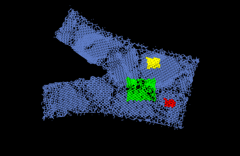
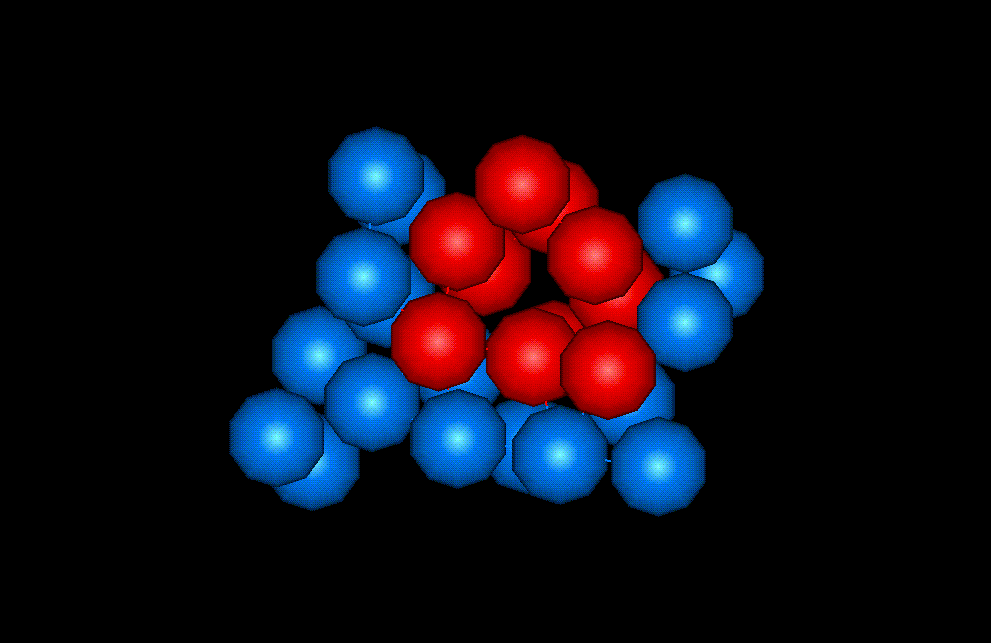
By selecting different regions of the material (refer to Figure 1), I was able to find two different crystal structures.
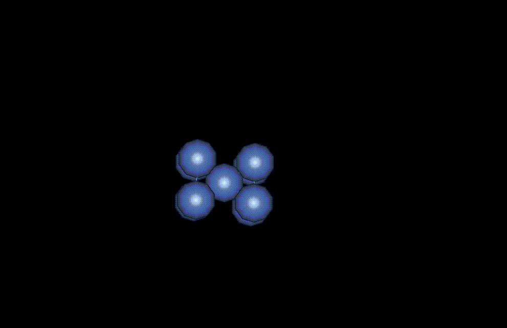
In the red region of Figure 1, I found what seems to be type of body centered cubic (Figure 2). But after measuring the bond angles and bond lengths the lattice doesn't appear to be cubic. It seems to be triclinic since none of the bond angles or bond lengths are equal.
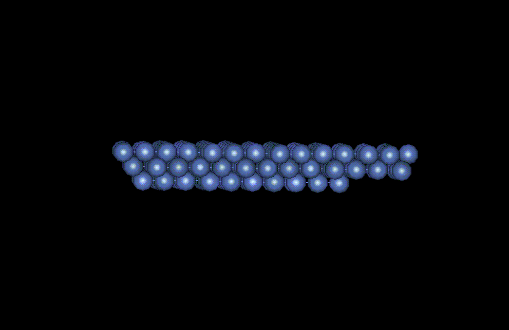
In the yellow region of Figure one, I found face centered cubic packing of the planes (Figure 3). The lattice parameter, a, was measured as 3.65 angstroms. If this is compared to the normal lattice parameter of nickel, 3.52 angstroms, it is clear that there is some bond stretching.
Specific Area Selected
The area that I selected is highlighted in green in Figure 1. The major crystal defects in this area are grain boundaries and vacancies. In the overall block of material there are not only grain boundaries and vacancies, but there are also stacking faults (caused by dislocations originating from the crack tip). If these defects are examined at a local level, they destroy the symmetry of the individual crystals, but if one takes a more macroscopic view of the defects, they do not destroy the overall symmetry of the entire piece of material being tested.
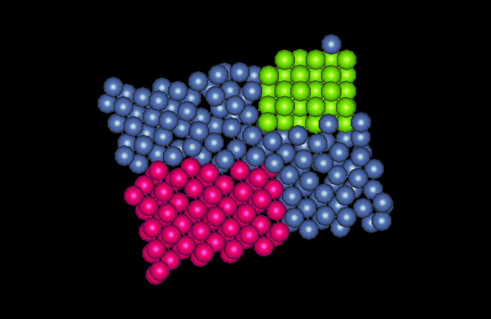
If one compares the green crystal and the fusca crystal in Figure 4, it is clear that they are oriented differently. So, one can measure the angle of disorientation caused by the grain boundary. This angle turns out to be approximately 147 degrees. In order to see the vacancy in this section of material, a zoomed view was necessary. So, if you examine Figure 5 in the area surrounded by red atoms, one can see that there might be a vacancy there.
The page was created by Matthew E. McMurtry for une in MSE 4948.
Date of Creation: September 9, 1998
Date of Most Recient Revision: September 11,
1998
Questions and Comments: mmcmurtr@vt.edu