Evaluation of Crystal Structures and Lattice Symmetries in a Nickel Film
David C. Haeberle
ESM 4984 Assignment 1
September 9, 1998
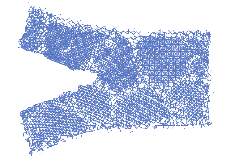
Nickel films are widely used due to their ability to withstand corrosion and high temperatures. Nickel is also a good electrical conductor, which makes nickel films an excellent candidate for electronics applications. Nickel films are also used in solar applications, chemical cells, battery applications, the aerospace industry, and in chemical processing. The basic structure of pure nickel is face-centered cubic (FCC) with a lattice parameter of 3.52 Angstroms. The region analyzed is a computer simulated nickel film with a crack propagating through the analysis region. The model, shown in Figure 1, only shows two planes of the atomic structure.
Figure 1: Nickel Film Crystal Structure
The unit cell of the crystal structure is defined by four sublattices, which describe the corners and faces of the FCC structure. The four sublattices are:
(0 0 0), (a/2, a/2, 0), (a/2, 0, a/2), (0, a/2, a/2).
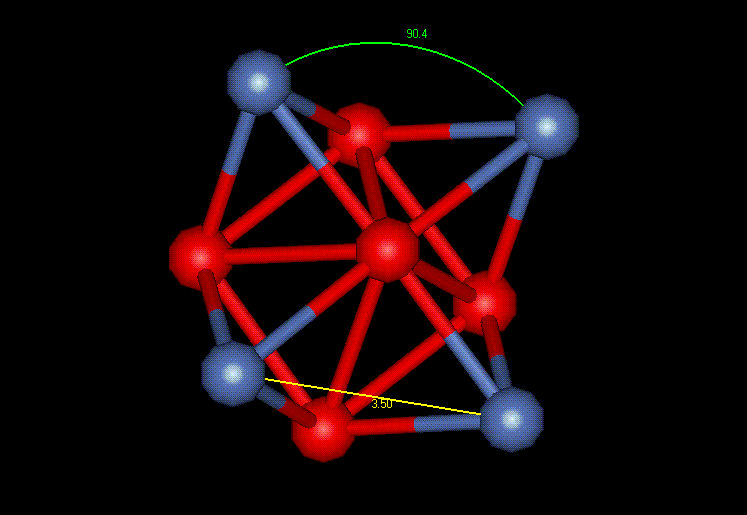
"a" is the lattice parameter of 3.52 Angstroms, thus making "a/2" equal to 1.76 Angstroms. Figure 2 shows a unit cell example extracted from a grain in the simulated nickel film. The blue atom represents a corner atom and the red atoms represent the face centers. 2.55, 2.53 and 2.53 Angstroms are the interatomic distances which correspond to the magnitude of sublattice vectors. The perfect lattice value is 2.49 Angstroms, very close to the measured values from the computer simulation. Using the unit cell shown in Figure 2, the rest of the crystal structure can be completed using symmetry. Figure 3 reveals more about the cubic FCC structure by showing two complete planes of a single cubic FCC crystal and the 45 and 90 degree angles necessary for the cubic classification. The lattice parameter, the distance between the corner atoms, is also noted (3.61 Angstroms). It is interesting to note that none of the crystals are "perfect" due to distances and angles slightly too large or too small.
Figure 2: FCC Unit Cell of Nickel
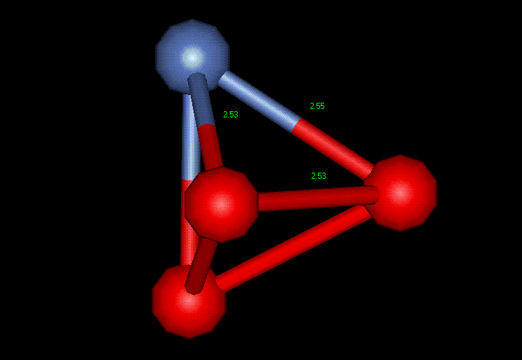
Figure 3: FCC Cubic Crystal Structure
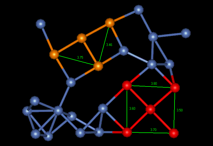
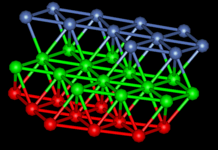
There are many grain boundaries, interfacial defects, associated with this nickel film. The boundaries are defined as areas separating two regions of having different crystallographic orientations. Figure 4 shows a grain boundary with its characteristic voids separating the grains of different orientation. The top of one FCC cubic crystal is represented by orange, and red represents a crystal at a different orientation. The two grains in this situation are offset by ten degrees.
Figure 4: Grain Boundary (Interfacial Defect)
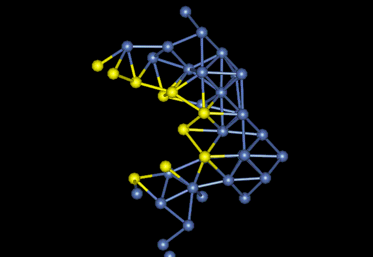
Another interesting area to look at in the crystal structure is the crack tip. At this point, bonds are being physically stretched until there is no longer any energy of attraction between the atoms, and then, they break apart. Measuring the bonds between the atoms in this region helps to identify what bond will break next as the crack progresses through the nickel film. Figure 5 shows the crack tip region. The yellow atoms represent the free surface of the crack. None of the bonds in this region appear to be stretched and about to break, but the crystal lattice structure is definitely distorted due to the crack propagation. The symmetry of the grain is definitely lost due to the crack.
Figure 5: Crack Tip
FCC crystal structures are a plane shift off of being hexagonal close-packed (HCP). It appears that in one instance a grain in the nickel film has slipped into the HCP form. This can be see by the 3 planes in Figure 6.
Figure 6: HCP Nickel
Summary:
The computer simulation of the nickel film really shows many of the defects associated with the imperfect material and crack propagation. Distorted crystals, interfacial defects, and HCP crystal structures were all located in the small element. The standard FCC crystal structure was located in most of the grains, but orientation differed from grain to grain.
References:
Bowman, Hamilton B. Handbook of Precision Sheet, Strip and Foil. American Society for Metals: Metals Park, OH, 1980.
Callister, William D. Jr. Materials Science and Engineering an Introduction. John Wiley & Sons, Inc.: New York, 1994.